
Helpful Hints for Hardware n00bs
Posted by FirmWarez on 27 Nov 2012 in Blog | 0 comments

Hardware is all the rage. Cool isn’t it? Hell yeah it’s cool. Like Dualcore’s “Natural 20s” cool.
Arduinos, Raspberry Pi, PICs, LEDs, CNC, robots, more folks are soldering at home than ever before.
I’ve been doing this a long time. Professionally a couple of decades. As a hobby much longer. I was probably 10 when I first handled an iron. I’ve had a lab essentially all my life. My first one was in a utility room, then the laundry room. Now I’ve got a huge workshop with a dedicated lab and machine shop.
People ask me all the time for advice. Makes my day really, all this creativity and building going on. I thought I’d put some of the most common questions and advice together in a blog to help folks get started. So here we go!
1) What soldering iron?
This is usually asked after people have done some soldering with a cheap hardware store iron. The big question is often “should I get a temperature controlled iron?” Maybe is the answer. What kind of soldering do you want plan on doing? I still keep some big ugly irons around for big ugly soldering, like automotive work. I do have a temperature controlled iron, but I find I usually use my small, brand name iron with a tiny tip. My big suggestion is no matter what, go for a good brand name, and use that manufacturers tips. You won’t go wrong with a Weller or Metcal. If you’re going to solder surface mount items, even more importantly than a temperature controlled iron is a good iron, a good, small tip, and good supplies, like solder. Just like the iron, match the solder to the work, small diameter solder for small parts.
2) What else for the solder bench?
ESD mat. Something to hold boards — a “third hand” or much much better yet a real “board clamp”. Flux. Flux cleaner. A sponge or other tip cleaner. Light, lots of light. Tweezers. An x-acto knife. Desoldering braid. Possibly a desoldering pump (I don’t use them much anymore personally). Magnification. At least a magnifying glass, some of the cheap ‘third hands’ come with them. Some folks like the big page size magnifying lamps; I have a really nice inspection (that is two objective lenses so 3D) microscope. Something heat resistant to protect your work surface. I use floor tiles, I mean they are like a buck each at Home Depot? Heat resistant ceramic tile, I feel so space-age. I keep a bottle of water on the bench for my sponges. I also keep a collection of trimmed component leads for jumpers and other such things. Alcohol wipes. Oh, and it’s not a bad idea to keep some saline solution close to your bench in case of eye contamination emergencies.
Another safety point. I’m a volunteer firefighter, and I have seen many people lose _everything_ in house fires. It is not fun. The lights on my solder bench and my irons are plugged in to the same power strip, a heavy duty one with a switch. I unplug the soldering iron, and turn off the strip. Lights are off, strip is off. I double check this every time I leave the lab. Trust me, while it is exciting to go in to a burning building, it’s not something I want to see happen.
Fume extraction. My lab is custom built, I have a bathroom type vent fan above the solder station. There are some nice little ‘fan and filter’ fume extractors. The fumes aren’t lead — soldering doesn’t get lead hot enough to go to vapor phase. Instead the fumes are from the flux, and can be irritating to eyes and respiratory system. Word of warning: flux fumes can trigger asthma in some folks. Considering the history of nerds and asthma, look out. But history is on our side: Teddy Roosevelt was an asthmatic smart guy with a nasally voice; he was also a total badass.
I’m a fan of special flux based tip cleaner things that clean and tin the tip. Tinning is coating the soldering iron tip with solder. The goal is to keep the tip from oxidizing. That’s what flux does, it helps get rid of oxides and contaminants so you are soldering clean metal. Oily, oxidized, contaminated metal won’t solder. Have a wire or part that just won’t solder? Flux it first. Keep your parts and tips clean. In extreme cases (like if I’ve been soldering nasty big automotive stuff) I will use a very sharp blade and gently scrape a solder tip. The flat grey gunk that comes off is called “dross”. It’s a collection of oxidized metal and flux and contamination remnants. Back in the day of solder wave machines for soldering large panels of through hole boards we would have to periodically clean the dross out of the solder pot. If you’ve never seen one, look it up. A “wave solder” is a big machine that pumps molten solder. Wicked cool.
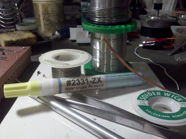
Solder bench regulars
3) How do you solder _some_tiny_package_ by hand?
Good tools (soldering iron, quality solder, flux, board holder, lighting, magnification, stuff I talked about above) and good skills. You get skills by working your way up. Most everyone starts with old fashioned “through hole parts”. Next is 1206 or 0805 surface mount discretes (resistors and capacitors) and SOIC chips. Small Outline IC. They have a lead pitch (the distance between pins) of 0.05″, as opposed to the 0.1″ of old DIP (Dual In-line Package) through hole chips.
To me SOIC seems huge anymore. Once you get good with those, you move on to TQFP and SSOP packages. Even smaller. It is possible to do QFN by hand. These don’t even have “leads”, the have solder points on the side of the device.
Some tricks? On fine pitch devices, use a flux pen on the pads and leads. This will make it easier to solder, and will help minimize bridging (solder sticking to more than one pin). I’ve seen highly skilled technicians put down flux and quickly solder these sorts of devices in seconds. I can’t do that. I try very carefully to solder pin by pin. Or I use desolder wick/braid. Flux the pads and part, solder as carefully as you can, then use the desolder wick to remove excess solder. It is very difficult to get all of the solder off the pins, which since you are putting the part down is what you want. Inspect for good solder joints and bridging under magnification.
QFN? The ones with the big center pad on the underside of the chip? I design my boards for such devices with a via in the middle of the center pad. Flux all the pads, get a little bit of solder on the lead pads. Flow some solder across the center pad, then put your iron on the back side of the board and heat that pad up. As small as these are, you will notice the lead pad solder is molten too. You’ve just turned your iron in to a small reflow system. Place the part on, and notice that it wants to orient itself correctly on the pads. You may have to help a little. Again, inspect for correct connections. Of course if you do tons of these things, maybe you should invest in a hot-air reflow system, or maybe a DIY reflow oven.
With any of the techniques, you can’t keep heat on the part forever, or you may damage it. Some parts are more sensitive than others. To get really good at placing small parts, you’ll have to practice. And probably kills some parts; be prepared for that. It is a skill, and like any skill, it doesn’t happen overnight.
No chlorine from these green dragons
3) How much should I worry about anti-static?
The classic engineering answer: it depends. Depends on what you’re handling. I’ve seen tests of PIC microcontrollers getting hit by automotive ignition coils causing nothing more than a reset. But then I’ve also been around things like true blue laser diodes that die if you look at them wrong. So, it depends. In general, the more complex a part, the more susceptible it is. Think about it like this: a high density chip, like say an ARM processor, compared to something old school, like a 555 (which I understand the photomasks were made with a technology called “crayon”), will have much much smaller features. That’s why all the new dense processors run on lower voltages than before, the features are physically smaller. That means it takes less ESD to damage the features.
For most stuff, just follow good practices. Have a grounded ESD work mat. Don’t handle parts until you are going to install them. Leave your parts and boards in anti-static bags. Ground yourself before handling parts. Don’t let nasty static sources, like styrofoam, anywhere near your work stations. Picking up and setting down a white styrofoam coffee cup can generate thousands of volts of electrostatic differential. Oh and guess what, if you can feel ESD, it’s really bad. Most of the discharges that can damage devices are imperceptible to humans.
Many of the parts used in maker projects (like microcontrollers) are designed to handle some rough environments. I mean the chip running your fuel injection controller in your car, a microcontroller, is in an ugly environment compared to your PC’s processor. It’s been a long time since I’ve seen a microcontroller die a confirmed ESD death. Again, other things, like laser diodes, are just flat-out sensitive.
Don’t be paranoid, just follow good practices. Oh, not to spread FUD, but most ESD failures are latent, that is they show up some time after the ESD event. That’s why some devices mysteriously just “die” after years in service. Latent ESD failure. You want to be paranoid? Design and handle stuff that goes in to airplanes or life-support equipment. Yes, I have, and yes, I can be paranoid when I need to be.
4) What about a power supply?
On the high end, you can get a really good bench supply which will have multiple outputs, variable voltage, variable current limit, built in meters, all very helpful. Among other uses, the variable current limit helps you from frying things in a first test. Set the current low so that if something is wrong you don’t get the full 5 amps or whatever your supply is capable of.
On the low end, you could just use a wall wart. But make sure it’s regulated. Many of them aren’t. If you use a non-regulated 5V wall wart on your 5V microcontroller project, it will probably end bad.
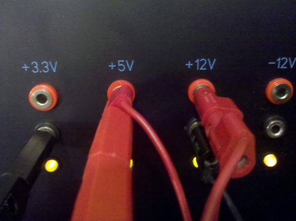
An option for many projects is to use a computer power supply. This gives you +3.3V, +5V, +12V, and -12V, which covers many home projects. Spark Fun has a board that allows you to easily connect to an ATX supply, however I wouldn’t advise using their board for high current projects because in my opinion the traces are too small.
Power supplies are like a lot of things. The question isn’t “what power supply should I get?” but rather “what power supply should I get for the projects I’m doing?” What voltages do you need? How much current?
In my lab I have a number of professional supplies with variable voltage and current limit, various mutli-voltage supply boards, rack mount supplies, and a collection of wall warts.
The usual suspects
5) Meters?
I’ve never owned a fancy high dollar Fluke or other similar meter. I’ve got a mid range meter that I use for most things. I only use the cheap multi-meters in the garage, where things are going to get dirty and banged around.
A good meter needs at least: volts, current, resistance, continuity. You will use the continuity feature quite a bit. Is this really connected? Are power and ground shorted? Does this switch still work? Continuity settings on meters usually beep, that is so helpful when testing these sorts of things.
It is handy to have multiple meters, for instance when you want to measure voltage across and current through something at the same time, like testing LEDs. I have a meter built in to a rack system that is one of my power supplies. I can measure the outputs of the supply, always handy to know that your assumptions are facts and not just assumptions. It can also measure outside voltages, so there’s an additional meter for general use.
6) What do I look for in a ‘scope?
For a beginner? Easy to use, reliable, cheap. There are some oscilloscopes out there that will do everything. I mean peak sampling, averaging, data acquisition everything. And they are nifty to have. But for a beginner, that can be overkill. Get something that matches your expected project range. If you’re a synth head and are just going to play with audio, a 20MHz o’scope is fine. Playing with microcontrollers? Kick it up to 100MHz. There are tons of inexpensive ‘scope options these days.
I will admit to having a bunch of old Tektronix ‘scopes around. My “go to” ‘scope for basic use is a Tek 465. Best damned o’scope ever made. Well, either that or I’ve been using them for so long they are just second nature for me.
Oh, and get good scope probes. Crappy probes on a good ‘scope is like 87 octane pump gas in an F1 engine: a bad idea. I use Probe Master probes, because they were basically down the street from a place I worked for in San Diego, and they have a great repair policy.
7) Why would I want a ‘scope?
Ok, so maybe you’ve done some basic troubleshooting with a multimeter. You can test continuity, voltage. You’re doing basic projects and want to know “what would I use a scope for?”
Well, anything that is changing rapidly. The classic first thing to check during microcontroller debugging is whether or not the clock is running. Since your oscillator may be 8MHz, 10MHz, or more, you won’t be able to tell with your voltmeter. But a quick probe with a scope and you’ll instantly know. Troubleshooting I2C, SPI, asynch serial, whatever communications? A scope can be handy. Again, you can instantly see bus collisions, clock glitches, and other issues. Running stepper motors? You can watch your control signals, and even (through a sense resistor) monitor your winding currents. The way a meter lets you see in to basic circuits, a scope lets you see in to anything happening quickly. Sound. Sensors. Oscillators. I even use mine for testing slow moving things, like say accelerometers. I’ve done a number of projects with very difficult to hand-solder QFN packaged accels. First thing I would do is power up the accel and probe the outputs with a scope. Wiggle the board, and you can see the signal wiggle — it’s much easier to visualize than trying to do the same with a voltmeter.
7) I really want to automate the world, how do?
Start small my friend. It’s very easy to get lost in a complex project. And it’s also very possible with hardware to deal with delayed gratification. Here’s what I mean. Want to learn programming? Download an environment like Python, type in print “hello world”, compile and run and wow, you have results! Want a custom circuit? Well, spec the parts. Draw the schematics. Do a layout. Order board and parts. Wait for parts to come in. Build board. Debug board…see what I mean? And if your board has errors, it’s not a case of hitting “compile” again. Hardware is time and money.
So start small. Blink an LED. Use pre-existing boards or designs, like an Arduino, or open source boards. Do some circuit bending. Build a kit. Your first projects should be simpler, so you can enjoy the success and the magic of watching something you’ve built work. It is incredible, even if it can be challenging. Don’t start off with overly complex. Build your way up. To make that uber project dream a reality, you need skills. Soldering skills. Debugging skills. Build your confidence and your skills.
There be dragons
9) Why won’t this work?
High side switching is more complicated than that. Inductive load without flyback diode. Not enough decoupling capacitance. Your traces are too small. You didn’t take frequency in to account. Ground loop. Signal to noise ratio. You need a dual rail op-amp. The inductor is saturated. The trace is too long. Plug-in proto boards are bad places to test high frequency circuits. Did you clean the flux off the board? In-rush current. You’re trying a time domain solution for a frequency domain problem. ADC input impedance.
Once you get past first order hardware projects, details can get critical.
10) There are all sorts of hardware_x. Which one is best?
The reason there are all sorts of x, is because there are all sorts of things you can do with x. So the answer is the standard engineering answer. It depends. The reason there are so many variants of everything is because once you’re past the first order solution, there are important details for different applications. So what you need to answer is “what is the best x for my application?” If you want to just learn? Go for low cost, easy to find.
11) What about schematic capture?
Well, I’m used to professional tools; I use Altium these days. I know Eagle is all street creddy, but the pros I know that use open source tools have gone to Kicad. The thing that really sucks about schematic capture is there is no magic dxf to go from one package to another. Yes, some packages will import/export, but it still is no where as easy as mechanical design. So get what you can, learn, but also understand that you can get kind of locked-in to the whatever your designs are in. Again, this is getting better, just be aware of it.
Nifty hax0rific video scanner
12) Do I need to learn anything special to do board layout?
Um, yeah. I mean basic layout is easy, but the best layout guys I know are people who have been doing it since the tape and mylar days. Yeah, that’s how they used to layout boards — red and blue tape over clear plastic. You put this stuff down by hand, red for the top and blue for the bottom, then took pictures of it with filters, reducing it, and then used those images for photomasks. Wow, crazy.
With complicated and not so complicated designs, there are all sorts of issues to consider when laying out a board. Board layout is not just about making parts fit and connecting signals. It’s where the physics of reality meet your design. Trace lengths, trace widths, location of capacitors, trace shapes, all of these things matter, and more. You will not be able to run a 10 amp motor with a 6-mil trace! It will vaporize. Other issues to think about include manufacturability. Right angles and acute angles can cause problems during the manufacturing process. Solder mask swell. Annular rings. Clearance swell on internal planes. It can get complicated in a hurry.
The nice thing about is is the board manufacturers will have guidelines, and there are all sorts of books and examples out there. On some critical parts the manufacturer’s datasheet will have example layouts — pay attention to what they are doing! There are reasons for these things. Again, it’s applied physics, and applied engineering. Like other hardware issues, start small. Build up your layout skills.
An important tip: DRC. Design Rules Check. Good layout software will let you set up rules, like min/max trace width, trace clearance, hole size. Run a DRC on your layout to check for shorts and other problems. Do it, ok? You don’t want to get a board back with power and ground shorted together, it’s bad, mmmkay? Oh min trace width/min clearance are referred to as “trace and space” in the biz. You may see a board house saying “6 mil trace and space”, that means you need 0.006″ between features and a minimum width of 0.006″. Mils. Thousandths of an inch.
Also it is helpful to “paper doll” your boards before spending good money on them. Print the copper layer at 1:1, and check for fit in the enclosure, fit of critical or difficult parts, collisions between parts, all that sort of thing. I still do this because no matter how good you are at visualizing what’s on the screen, it looks different as real hardware. You’ll find wasted space and crowded parts, so do it. Think about the fact that you will be placing the parts. Sure, you can fit them that close together, but how will you solder them in place? A paper doll helps with these questions and more.

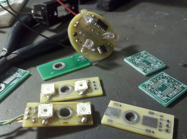
World’s smallest LED cube?
13) PCB? Buy? Make? What kind?
It can be an interesting experience to etch your own board. I got started doing that in the #wayback. There are also some nifty CNC routing methods of making boards, but these days, I buy. There are many inexpensive, cheap, and super cheap board houses. Use these. Typically thicker two sided boards are your cheapest route. Two sided means there are traces on the top and bottom of the board. More complex than that are multilayer boards, that have traces and planes (big chunks of copper for power and ground) laminated _inside_ the boards. Yes, these are more expensive. And they have some other difficulties — like if you have a mistake on an internal plane you may be totally hosed. Start off with double-sided boards. Many times I even choose to leave off the soldermask on prototypes, because it makes it easier to probe signals, cut traces, and add jumpers/parts if necessary.
The “green” stuff on boards is the soldermask. Yes, lot’s of people are now using different colors. I’ve done that forever, with black soldermask for display boards so they hide behind say LEDs, or different colored soldermask for different revisions of protoptypes. Purple for first rev (p is for purple, p is for prototype), different colors if we had other protos, saving the (cheaper) green for production. I’ve also done products that went in to clear enclosures where the board color indicated the type of product (like the color of the LED). Get creative.
Soldermask is not there to “protect” the board. It sort of does, but it’s there to keep solder from sticking to places it shouldn’t. That’s how high density parts solder correctly in reflow ovens — the soldermask prevents bridging. Want proof that soldermask doesn’t protect? Look at something designed for a difficult environment, like a hot tub controller (I’ve designed some of these). It will have a shiny thick layer of gunk over the board. Called “conformal coating”, this is how you protect a board against moisture and so forth. One brand is called “Humiseal“, it is thick and sticky; called “human seal” by an engineer I used to work with who never seemed to be able to conformal coat boards without conformal coating himself.
Something else you have to think about when ordering boards is whether you want “silkscreen”. These are the usually white or yellow markings of component designators, etc. Very helpful, but some board houses charge extra on prototypes, or at least extra for bottom side silk. Do make sure your silkscreen layer stuff is not over your solder pads for components, that’s a n00b mistake.
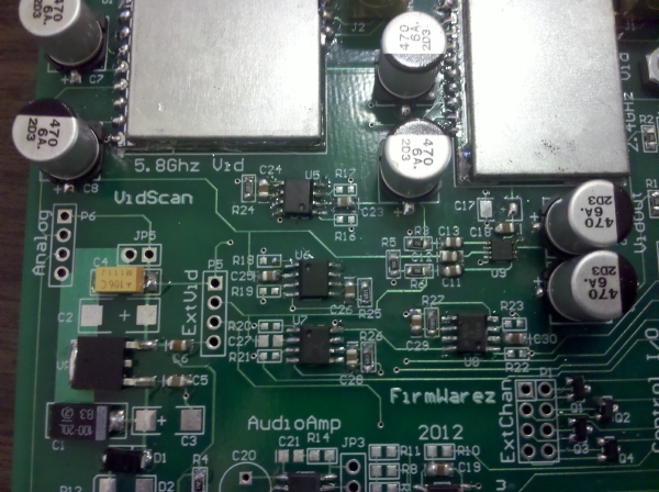
Also, add text to your boards. Your hacker handle, the year, what the board is. It’s handy if somepony takes a picture of your board and posts it for the whole net to see. (even if the “FirmWarez” part is blurry. Arg.) It’s also handy to remember what the board is supposed to be, and what revision it is in case you make changes. Even if you don’t do silkscreen, you can add text to the copper layer. Or do like I do sometimes, the same text on copper and silk slightly offset so you get this cool 3D shadow look.
—————————————
Working with hardware is fun and rewarding. It can also be frustrating and expensive. I will reiterate: start with a few projects that have almost determined success to minimize frustration. Then go out there and build. And build some more. Learn new skills, make crazy new things, and share your ideas, experiences, and designs.
Wow, so because of a few questions folks have asked me here and there, I’ve written my longest blog entry to date. Please feel free to ask me questions; my e-mail is not hard to figure out.